
Breadboard


A breadboard, solderless breadboard, or protoboard is a construction base used to build semi-permanent prototypes of electronic circuits. Unlike a perfboard or stripboard, breadboards do not require soldering or destruction of tracks and are hence reusable. For this reason, breadboards are also popular with students and in technological education.
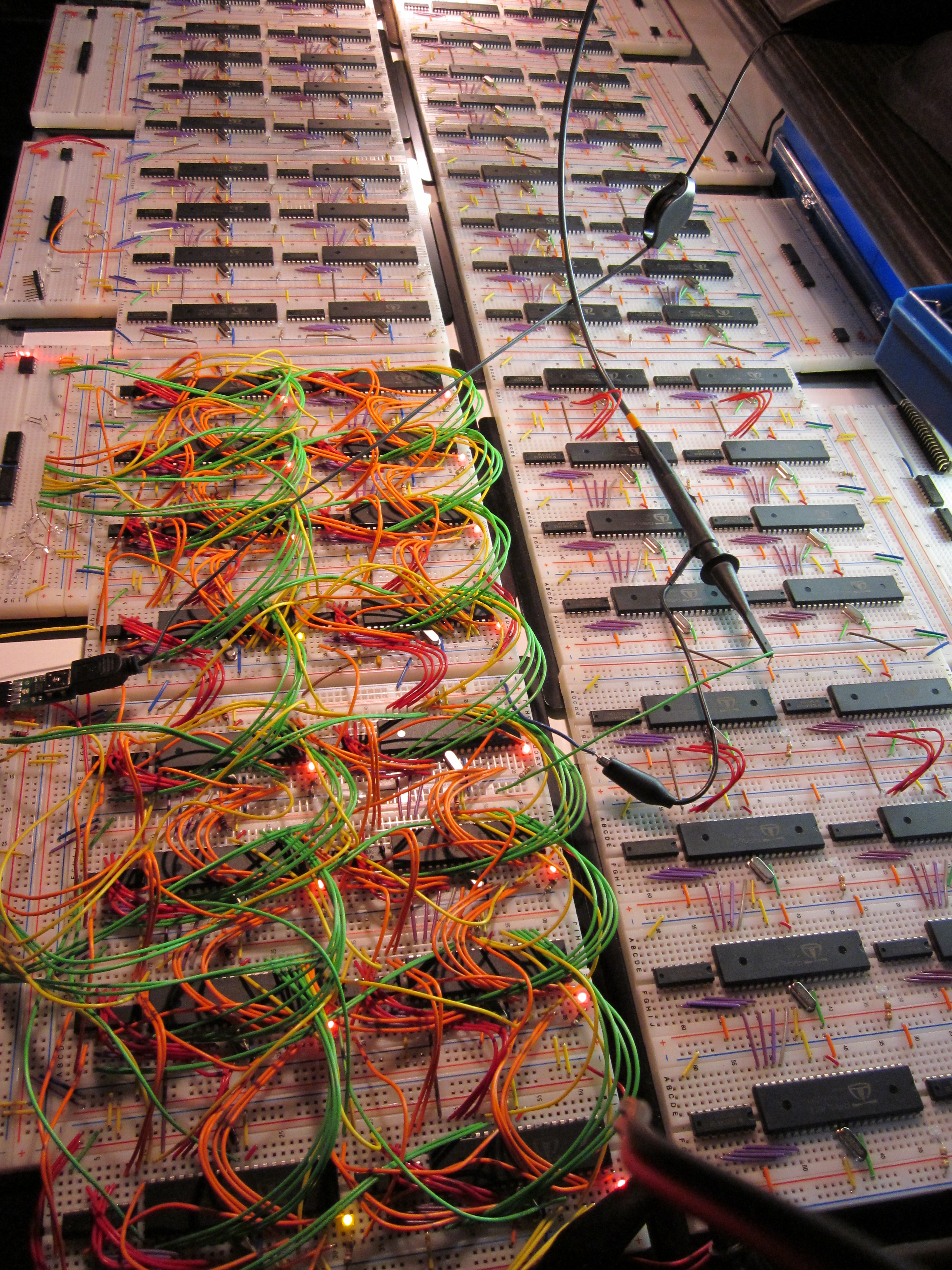
A variety of electronic systems may be prototyped by using breadboards, from small analog and digital circuits to complete central processing units (CPUs).
Compared to more permanent circuit connection methods, modern breadboards have high parasitic capacitance, relatively high resistance, and less reliable connections, which are subject to jostle and physical degradation. Signaling is limited to about 10 MHz, and not everything works properly even well below that frequency.
History[edit]

In the early days of radio, amateurs nailed bare copper wires or terminal strips to a wooden board (often literally a bread cutting board) and soldered electronic components to them.[1] Sometimes a paper schematic diagram was first glued to the board as a guide to placing terminals, then components and wires were installed over their symbols on the schematic. Using thumbtacks or small nails as mounting posts was also common.
Breadboards have evolved over time with the term now being used for all kinds of prototype electronic devices. For example, US Patent 3,145,483,[2] was filed in 1961 and describes a wooden plate breadboard with mounted springs and other facilities. US Patent 3,496,419,[3] was filed in 1967 and refers to a particular printed circuit board layout as a Printed Circuit Breadboard. Both examples refer to and describe other types of breadboards as prior art.
In 1960, Orville Thompson of DeVry Technical Institute patented a solderless breadboard connecting rows of holes together with spring metal.[4] In 1971, Ronald Portugal of E&L Instruments patented a similar concept with holes in 0.1 inches (2.54 mm) spacings, the same as DIP IC packages, which became the basis of the modern solderless breadboard that is commonly used today.[5]
Prior art[edit]
- US Patent 231708, filed in 1880, "Electrical switch board".[6]
- US Patent 2477653, filed in 1943, "Primary electrical training test board apparatus".[7]
- US Patent 2592552, filed in 1944, "Electrical instruction board".[8]
- US Patent 2568535, filed in 1945, "Board for demonstrating electric circuits".[9]
- US Patent 2885602, filed in 1955, "Modular circuit fabrication", National Cash Register (NCR).[10]
- US Patent 3062991, filed in 1958, "Quick attaching and detaching circuit system".[11]
- US Patent 2983892, filed in 1958, "Mounting assemblage for electrical circuits".[12]
- US Patent 3085177, filed in 1960, "Device for facilitating construction of electrical apparatus", DeVry Technical Institute.[4]
- US Patent 3078596, filed in 1960, "Circuit assembly board".[13]
- US Patent 3145483, filed in 1961, "Test board for electronic circuits".[2]
- US Patent 3277589, filed in 1964, "Electrical experiment kit".[14]
- US Patent 3447249, filed in 1966, "Electronic building set".[15] See Lectron blocks / dominoes.
- US Patent 3496419, filed in 1967, "Printed circuit breadboard".[3]
- US Patent 3540135, filed in 1968, "Educational training aids".[16]
- US Patent 3733574, filed in 1971, "Miniature tandem spring clips", Vector Electronics.[17][18]
- US Patent D228136, filed in 1971, "Breadboard for electronic components or the like", E&L Instruments.[5][19][20] This is the modern solderless breadboard.
Design[edit]

A modern solderless breadboard socket consists of a perforated block of plastic with numerous tin plated phosphor bronze or nickel silver alloy spring clips under the perforations. The clips are often called tie points or contact points. The number of tie points is often given in the specification of the breadboard.
The spacing between the clips (lead pitch) is typically 0.1 inches (2.54 mm). Integrated circuits (ICs) in dual in-line packages (DIPs) can be inserted to straddle the centerline of the block. Interconnecting wires and the leads of discrete components (such as capacitors, resistors, and inductors) can be inserted into the remaining free holes to complete the circuit. Where ICs are not used, discrete components and connecting wires may use any of the holes. Typically the spring clips are rated for 1 ampere at 5 volts and 0.333 amperes at 15 volts (5 watts).
Bus and terminal strips[edit]

Solderless breadboards connect pin to pin by metal strips inside the breadboard. The layout of a typical solderless breadboard is made up from two types of areas, called strips. Strips consist of interconnected electrical terminals. Often breadboard strips or blocks of one brand have male and female dovetail notches so boards can be clipped together to form a large breadboard.
The main areas, to hold most of the electronic components, are called terminal strips. In the middle of a terminal strip of a breadboard, one typically finds a notch running in parallel to the long side. The notch is to mark the centerline of the terminal strip and provides limited airflow (cooling) to DIP ICs straddling the centerline[citation needed]. The clips on the right and left of the notch are each connected in a radial way; typically five clips (i.e., beneath five holes) in a row on each side of the notch are electrically connected. The five columns on the left of the notch are often marked as A, B, C, D, and E, while the ones on the right are marked F, G, H, I and J. When a "skinny" dual in-line pin package (DIP) integrated circuit (such as a typical DIP-14 or DIP-16, which have a 0.3-inch (7.6 mm) separation between the pin rows) is plugged into a breadboard, the pins of one side of the chip are supposed to go into column E while the pins of the other side go into column F on the other side of the notch. The rows are identified by numbers from 1 to as many the breadboard design goes. A full-size terminal breadboard strip typically consists of around 56 to 65 rows of connectors. Together with bus strips on each side this makes up a typical 784 to 910 tie point solderless breadboard. Most breadboards are designed to accommodate 17, 30 or 64 rows in the mini, half, and full configurations respectively.
To provide power to the electronic components, bus strips are used. A bus strip usually contains two columns: one for ground and one for a supply voltage. However, some breadboards only provide a single-column power distribution bus strip on each long side. Typically the row intended for a supply voltage is marked in red, while the row for ground is marked in blue or black. Some manufacturers connect all terminals in a column. Others just connect groups of, for example, 25 consecutive terminals in a column. The latter design provides a circuit designer with some more control over crosstalk (inductively coupled noise) on the power supply bus. Often the groups in a bus strip are indicated by gaps in the color marking. Bus strips typically run down one or both sides of a terminal strip or between terminal strips. On large breadboards additional bus strips can often be found on the top and bottom of terminal strips.
.jpg)
Some manufacturers provide separate bus and terminal strips. Others just provide breadboard blocks which contain both in one block.
Jump wires[edit]

Jump wires (also called jumper wires) for solderless breadboarding can be obtained in ready-to-use jump wire sets or can be manually manufactured. The latter can become tedious work for larger circuits. Ready-to-use jump wires come in different qualities, some even with tiny plugs attached to the wire ends. Jump wire material for ready-made or homemade wires should usually be 22 AWG (0.33 mm2) solid copper, tin-plated wire - assuming no tiny plugs are to be attached to the wire ends. The wire ends should be stripped 3⁄16 to 5⁄16 in (4.8 to 7.9 mm). Shorter stripped wires might result in bad contact with the board's spring clips (insulation being caught in the springs). Longer stripped wires increase the likelihood of short-circuits on the board. Needle-nose pliers and tweezers are helpful when inserting or removing wires, particularly on crowded boards.
Differently colored wires and color-coding discipline are often adhered to for consistency. However, the number of available colors is typically far fewer than the number of signal types or paths. Typically, a few wire colors are reserved for the supply voltages and ground (e.g., red, blue, black), some are reserved for main signals, and the rest are simply used where convenient. Some ready-to-use jump wire sets use the color to indicate the length of the wires, but these sets do not allow a meaningful color-coding schema.
Advanced designs[edit]
In a more robust variant, one or more breadboard strips are mounted on a sheet of metal. Typically, that backing sheet also holds a number of binding posts. These posts provide a clean way to connect an external power supply. This type of breadboard may be slightly easier to handle.
Some manufacturers provide high-end versions of solderless breadboards. These are typically high-quality breadboard modules mounted on a flat casing. The casing contains additional equipment for breadboarding, such as a power supply, one or more signal generators, serial interfaces, LED display or LCD modules, and logic probes.[21]
For high-frequency development, a metal breadboard affords a desirable solderable ground plane, often an unetched piece of printed circuit board; integrated circuits are sometimes stuck upside down to the breadboard and soldered to directly, a technique sometimes called "dead bug" construction because of its appearance. Examples of dead bug with ground plane construction are illustrated in a Linear Technologies application note.[22]
Uses[edit]
A common use in the system on a chip (SoC) era is to obtain an microcontroller (MCU) on a pre-assembled printed circuit board (PCB) which exposes an array of input/output (IO) pins in a header suitable to plug into a breadboard, and then to prototype a circuit which exploits one or more of the MCU's peripherals, such as general-purpose input/output (GPIO), UART/USART serial transceivers, analog-to-digital converter (ADC), digital-to-analog converter (DAC), pulse-width modulation (PWM; used in motor control), Serial Peripheral Interface (SPI), or I²C.
Firmware is then developed for the MCU to test, debug, and interact with the circuit prototype. High frequency operation is then largely confined to the SoC's PCB. In the case of high speed interconnects such as SPI and I²C, these can be debugged at a lower speed and later rewired using a different circuit assembly methodology to exploit full-speed operation. A single small SoC often provides most of these electrical interface options in a form factor barely larger than a large postage stamp, available in the American hobby market (and elsewhere) for a few dollars, allowing fairly sophisticated breadboard projects to be created at modest expense.
Limitations[edit]


Due to relatively large parasitic capacitance compared to a properly laid out PCB (approx 2 pF between adjacent contact columns[23]), high inductance of some connections and a relatively high and not very reproducible contact resistance, solderless breadboards are limited to operation at relatively low frequencies, usually less than 10 MHz, depending on the nature of the circuit. The relatively high contact resistance can already be a problem for some DC and very low frequency circuits. Solderless breadboards are further limited by their voltage and current ratings.
Solderless breadboards usually cannot accommodate surface-mount technology devices (SMD) or components with grid spacing other than 0.1 inches (2.54 mm). Further, they cannot accommodate components with multiple rows of connectors if these connectors do not match the dual in-line layout—it is impossible to provide the correct electrical connectivity. Sometimes small PCB adapters called "breakout adapters" can be used to fit the component to the board. Such adapters carry one or more components and have 0.1 inches (2.54 mm) spaced male connector pins in a single in-line or dual in-line layout, for insertion into a solderless breadboard. Larger components are usually plugged into a socket on the adapter, while smaller components (e.g., SMD resistors) are usually soldered directly onto the adapter. The adapter is then plugged into the breadboard via the 0.1 in (2.54 mm) connectors. However, the need to solder the components onto the adapter negates some of the advantage of using a solderless breadboard.
Very complex circuits can become unmanageable on a solderless breadboard due to the large amount of wiring required. The very convenience of easy plugging and unplugging of connections also makes it too easy to accidentally disturb a connection, and the system becomes unreliable. It is possible to prototype systems with thousands of connecting points, but great care must be taken in careful assembly, and such a system becomes unreliable as contact resistance develops over time. At some point, very complex systems must be implemented in a more reliable interconnection technology, to have a likelihood of working over a usable time period.
Alternatives[edit]
Alternative methods to create prototypes are point-to-point construction (reminiscent of the original wooden breadboards), wire wrap, wiring pencil, and boards like the stripboard. Complicated systems, such as modern computers comprising millions of transistors, diodes, and resistors, do not lend themselves to prototyping using breadboards, as their complex designs can be difficult to lay out and debug on a breadboard.
Modern circuit designs are generally developed using a schematic capture and simulation system, and tested in software simulation before the first prototype circuits are built on a printed circuit board. Integrated circuit designs are a more extreme version of the same process: since producing prototype silicon is costly, extensive software simulations are performed before fabricating the first prototypes. However, prototyping techniques are still used for some applications such as RF circuits, or where software models of components are inexact or incomplete.
It is also possible to use a square grid of pairs of holes where one hole per pair connects to its row and the other connects to its column. This same shape can be in a circle with rows and columns each spiraling opposite clockwise/counterclockwise.
See also[edit]
References[edit]
- ^ Description of the term breadboard Archived 2007-09-27 at the Wayback Machine
- ^ a b U.S. Patent 3145483. Archived 2018-01-23 at the Wayback Machine: "Test board for electronic circuits", filed 4 May 1961, retrieved 14 July 2017.
- ^ a b U.S. Patent 3496419. Archived 2018-01-23 at the Wayback Machine: "Printed circuit breadboard", filed 25 Apr 1967, retrieved 14 July 2017.
- ^ a b U.S. Patent 3085177. Archived 2018-01-23 at the Wayback Machine: "Device for facilitating construction of electrical apparatus", filed 7 Jul 1960, retrieved 14 Jan 2017.
- ^ a b U.S. Patent D228136.: "Breadboard for electronic components or the like", filed 1 Dec 1971, retrieved 14 July 2017.
- ^ U.S. Patent 231708. "Electrical switch board", filed 31 Aug 1880, retrieved 4 August 2019.
- ^ U.S. Patent 2477653. Archived 2018-01-23 at the Wayback Machine: "Primary electrical training test board apparatus", filed 10 Apr 1943, retrieved 14 July 2017.
- ^ U.S. Patent 2592552. "Electrical instruction board", filed 4 Oct 1944, retrieved 23 Oct 2022.
- ^ U.S. Patent 2568535. Archived 2018-01-23 at the Wayback Machine: "Board for demonstrating electric circuits", filed 10 Apr 1945, retrieved 14 July 2017.
- ^ U.S. Patent 2885602.: "Modular circuit fabrication", filed 4 Apr 1955, retrieved 14 July 2017.
- ^ U.S. Patent 3062991. Archived 2018-01-23 at the Wayback Machine: "Quick attaching and detaching circuit system", filed 8 Sep 1958, retrieved 14 July 2017.
- ^ U.S. Patent 2983892. Archived 2018-01-23 at the Wayback Machine: "Mounting assemblage for electrical circuits", filed 14 Nov 1958, retrieved 14 July 2017.
- ^ U.S. Patent 3078596. Archived 2018-01-23 at the Wayback Machine: "Circuit assembly board", filed 21 Nov 1960, retrieved 14 Jan 2017.
- ^ U.S. Patent 3277589. Archived 2018-01-23 at the Wayback Machine: "Electrical experiment kit", filed 5 Nov 1964, retrieved 14 July 2017.
- ^ U.S. Patent 3447249.: "Electronic building set", filed 5 May 1966, retrieved 14 Jan 2017.
- ^ U.S. Patent 3540135.: "Educational training aids", filed 11 Oct 1968, retrieved 14 July 2017.
- ^ U.S. Patent 3733574.: "Miniature tandem spring clips", filed 23 Jun 1971, retrieved 14 Jan 2017.
- ^ Vector Electronics and Technology; Company Website.
- ^ E&L Instruments in Open Database Of The Corporate World.
- ^ "wire stripper". Retrieved 14 April 2023.
- ^ Powered breadboard Archived 2011-10-09 at the Wayback Machine
- ^ Linear Technology (August 1991). "Application Note 47: High Speed Amplifier Techniques" (pdf). Retrieved 2016-02-14. Dead-bug breadboards with ground plane, and other prototyping techniques, illustrated in Figures F1 to F24, from p. AN47-98. There is information on breadboarding on pp. AN47-26 to AN47-29.
- ^ Jones, David. "EEVblog #568 - Solderless Breadboard Capacitance". EEVblog. Archived from the original on 21 January 2014. Retrieved 15 January 2014.
External links[edit]
| Authority control databases: National |
|---|